started 27th June 2016
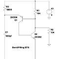
PUT part 1 discussed the programmable unijunction transistor (PUT) oscillator - by this I mean a complementary pair of transistors with feedback, rather than a real unijunction transistor. See also Phase Noise, PUT3.
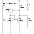
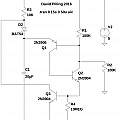
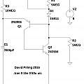
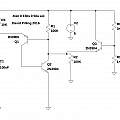
The shortcoming of the standard circuit is that the two resistors on the right hand side forming a potential divider have to be a lot smaller than the resistor on the left which charges the capacitor - wasting power. I showed an improved circuit which uses an extra transistor as part of a current mirror and allows the right hand resistors to be around the same value as the one on the left.
First graphic standard circuit, second improved version.
Low current LED flasher
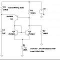
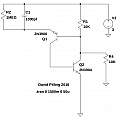
This variation of the low current version flashes an LED. Average current consumption is 5 μA. However efficiency (power that ends up in the LED against power consumption) is only about 20%; more power ends up in the resistor used to charge the capacitor than the LED.
The LED would flash brighter if the current charging the capacitor was greater (because for a given period the capacitor could be bigger), this means the resistor on the left being smaller than the ones on the right. The above PUT circuits won't work in this configuration but the following one will.
Non-stick PUT oscillators
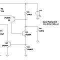
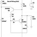
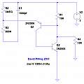
PUT circuits stop oscillating when the conducting state becomes stable, this happens if the current through R3 is great enough and Q2 saturates. The idea of this circuit is that a third transistor, Q3, stops the current through R3 in the conducting state.
This is a version using a diode to switch off the current through R3, the output is close to a square wave. Looking back, there is a comparison to make with Richard Torren's Trafficator flasher circuit, which in turn uses a diode in the same way as the design from the "Handbook of Semiconductor Circuits" published in 1960, shown at the bottom of this page. There Q3 connects to the other end of the diode.
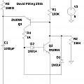
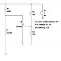
Another version, coming from the Phase Noise idea of letting the capacitor charge from a voltage close to the threshold. Uses one extra diode and can work with low current (less than 1 μA for the values below).
Clamped PUT oscillators
A way of avoiding transistor saturation is the "Baker Clamp". These three graphics show variations applied to the PUT oscillator. The third one is the most effective but at the cost of higher power consumption.
LT Spice file of the first circuit
LT Spice file of the second circuit
LT Spice file of the third circuit
Upside down PUT oscillator
The capacitor can be put in parallel with the resistor. In this case the capacitor charges via Q1 and discharges through the resistor R2.
A version of the upside down circuit that generates squareish waves.
Faster, faster...
The standard PUT oscillator won't work at high frequencies, due to the high value of R3 forcing small capacitor values. The modified circuits above will more easily go faster. This reminded me that I built R A Penfold's transistor oscilloscope from the December 1972 and January 1973 Radio Constructor (available here). The time-base oscillator in that was designed around the TIS43 (a genuine Unijunction not a PUT) and operated at up to 500 KHz.
The Real Thing (or not)
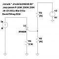
A circuit using a real PUT, the 2N6027. Useful references were:
The Unijunction Transistor (UJT) - All About Circuits
Unijunction transistor in LTspice? - Electrical Engineering Stack Exchange
My ebay sourced 2N6027 didn't work; using an AVR transistor tester (available in many versions based on this open hardware project - which recognises lots of different components), revealed it was a thyristor with the opposite order connections to the data sheet; it still didn't work when rotated.
So I bought some 2N6028 off ebay; the AVR tester said these were PNP transistors; but they did work nicely in the above circuit.
I found that the second edition of The Art of Electronics by Horowitz and Hill (1989) devotes chapter 14 to low power design and one example (figure 14.36) is an oscillator using the 2N6028 which will run off 1 μA. Part of the circuit is shown below, the output can be taken from the junction of R4 and the 2N6028.
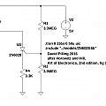
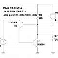
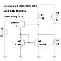
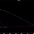
Much of the discussion around picking resistors for the real PUT is centred around the current voltage curve for the device. I got LT Spice to plot similar curves for various circuits. The graphics show the circuits, 2N6028, complementary pair PUT and current mirror PUT.
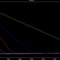
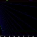
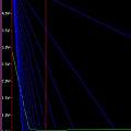
The next graphics show the corresponding results. The resistors on the right (R1 and R2) are equal and stepped from 100K to 2M in 200K steps. The curve for the smallest resistance value is the rightmost one.
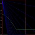
At the far left, zero voltage gives zero current. There is then a rapid rise of voltage with little current flowing. Once the peak voltage is reached the device turns on, with voltage decreasing as current increases, this is the zone of 'negative (dynamic) resistance'. Eventually, past the valley bottom, increasing current requires higher voltage.
The curve is similar to that of the Pearson–Anson effect, which, discovered in 1922, is the oscillation produced by a neon bulb connected across a capacitor, when a direct current is applied through a resistor. According to the Wikipedia article, for oscillation to occur the load line of the resistor must pass through the negative resistance part of the current voltage curve.
Graphics show current voltage curves (green), negative resistance zone (area under the red curve) and load lines (blue). The resistance for the load lines steps from 100K to 3000K in 200K steps; the smallest resistance is rightmost. For the 2N6028 the value of R1 and R2 is 300K. For the current mirror R1 and R2 have value 2M. For the complementary pair R1 and R2 have value 10K,
LT Spice files to produce the last two sets of three graphics
The conclusion is the same as the original qualitative arguments, the current mirror PUT can work with a smaller ratio of the resistor on the left to the two on the right. But the graphs show the acceptable range of values.
Negative resistance references
Negative Resistance Devices Graphical Analysis and Load Lines
Oscillations and Regenerative Amplification using Negative Resistance
A Dip Meter Using the Lambda Negative Resistance Circuit
Lambda Diodes
Negative resistance VCO
NEGATIVE RESISTANCE AND THE LAMBDA DIODE
FUN WITH NEGATIVE RESISTANCE: JELLYBEAN TRANSISTORS
Comments
