PUT
The programmable unijunction transistor (PUT) oscillator is discussed here:
Discrete Sawtooth Oscillators Alan Yates
PUT Complimentary Feedback Pair 4QD/Richard Torrens
See also PUT part 2, PhaseNoise and PUT part3.
The term PUT is being used here to describe combining two discrete transistors to emulate a programmable unijunction transistor.
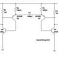
Shown below is the typical PUT oscillator. Increasing the resistors R1 and R2 in an attempt to reduce the power usage stops oscillation.
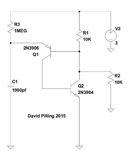
Starting with both transistors turned off, the voltage at the emitter of Q1 increases as C1 charges via R3 until it is around Vbe greater than the voltage at the base of Q1 (set by R1 and R2), at that point Q1 begins to conduct and the resulting current through the base of Q2 causes it to also start conducting pulling the base of Q1 down further. A rapid drop in the voltage at the junction of R1 and R2 follows, along with the discharge of C1.
This phase gives the characteristic very sharp drop in voltage.
The state of both transistors turned fully on is stable (and there will be no oscillation) unless the current through R3 is insufficient to keep Q2 fully turned on. In other words if Q2 is saturated by the current through R3 oscillation will not take place. This is why a low value for R1 (relative to R3) is necessary for the standard version of the circuit to work.
An increase in the voltage at the collector of Q2 will reduce the base current of Q1 reducing its collector current and the base current of Q2 and so on.
By reducing the value of R1 the return of the voltage at the collector of Q2 to the value set by R1 and R2 is made faster.
Low current circuit
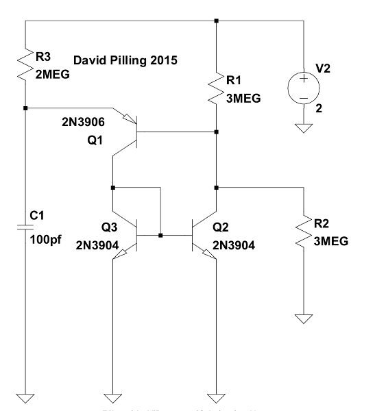
This is a version which when built used 1 μA; Q2 and Q3 are a current mirror.
After changing the resistors to 10 MΩ and the power supply voltage to 1.2 V it used 130 nA. Roughly a load of 10 MΩ on the power supply.
If I touch the input of my 'scope with my finger it shows a 50 Hz wave with amplitude 11 V pp. This is the common "mains hum" phenomena. Removing the power supply from the circuit and touching the positive rail, supplies enough power from this source to make it oscillate.
For the low current version to work various conditions have to be met.
The emitter of Q1 has to get Vbe above its base. Which implies V2 R1 / (R1+R2) > Vbe.
A rough calculation is that in the conducting state when the capacitor has discharged the current through R3 will be mirrored through R1 if
R1 (V2-Vbe)/R3 < V2
and the state will not be stable. However all that is necessary is for a reduction in current through Q3 to give a reduction in current through Q2; which means the circuit will work with values that don't meet the above condition. But if R1 is too big relative to R3 the circuit will not leave the conducting state. This does echo the problem with the original PUT oscillator but ratio of the resistors can be much smaller; because the gain of a transistor is replaced with the gain of the current mirror which is unity. See PUT part 2 for a configuration that allows R3 to be much less than R1.
Another version of this circuit with a period of over two hours and current consumption of 0.2 μA can be used to trigger a micro-controller, see Waking from sleep mode.
Other low current oscillators:
3 nA oscillator by Dave Johnson
microamp oscillators by Dave Johnson
Low Voltage Micropower LC (Colpitts) Oscillator Circuit with Active Load, Advanced Linear Devices
Square wave oscillator
This reference shows how to use two unijunction transistors to produce a square wave
Getting to Know the UJT April 1970 Popular Electronics By Frank H. Tooker
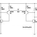
The same configuration works using the PUT. Click to see large image.
The turn off mechanism is different to the usual PUT circuit, it does not rely on the NPN transistor not being saturated, the result is that this circuit can be used with high value resistors. Click to see large image.
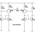
The configuration works better at low currents with the current mirror version of the PUT. The one shown uses around 1 μA and produces a somewhat square wave output. Click to see large image.
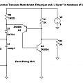
I found another way to generate a square wave in "Handbook of Semiconductor Circuits" (published originally as "Military Standardization Handbook, Selected Semiconductor Circuits, MIL-HDBK-215" in 1960). This uses an extra diode to increase the time the capacitor takes to discharge. Whilst C1 is charging, things go as in the standard circuit at the top of this page; once Q1 turns on, the diode D1 is reverse biased and C1 cannot discharge (quickly) through Q1, instead it discharges (slowly) through R4.
Click to see large image.
Adding a single resistor to the basic circuit produces squareish wave.
Click to see large image.
David Pilling's Wiki
Set view
